AI-generated illustration
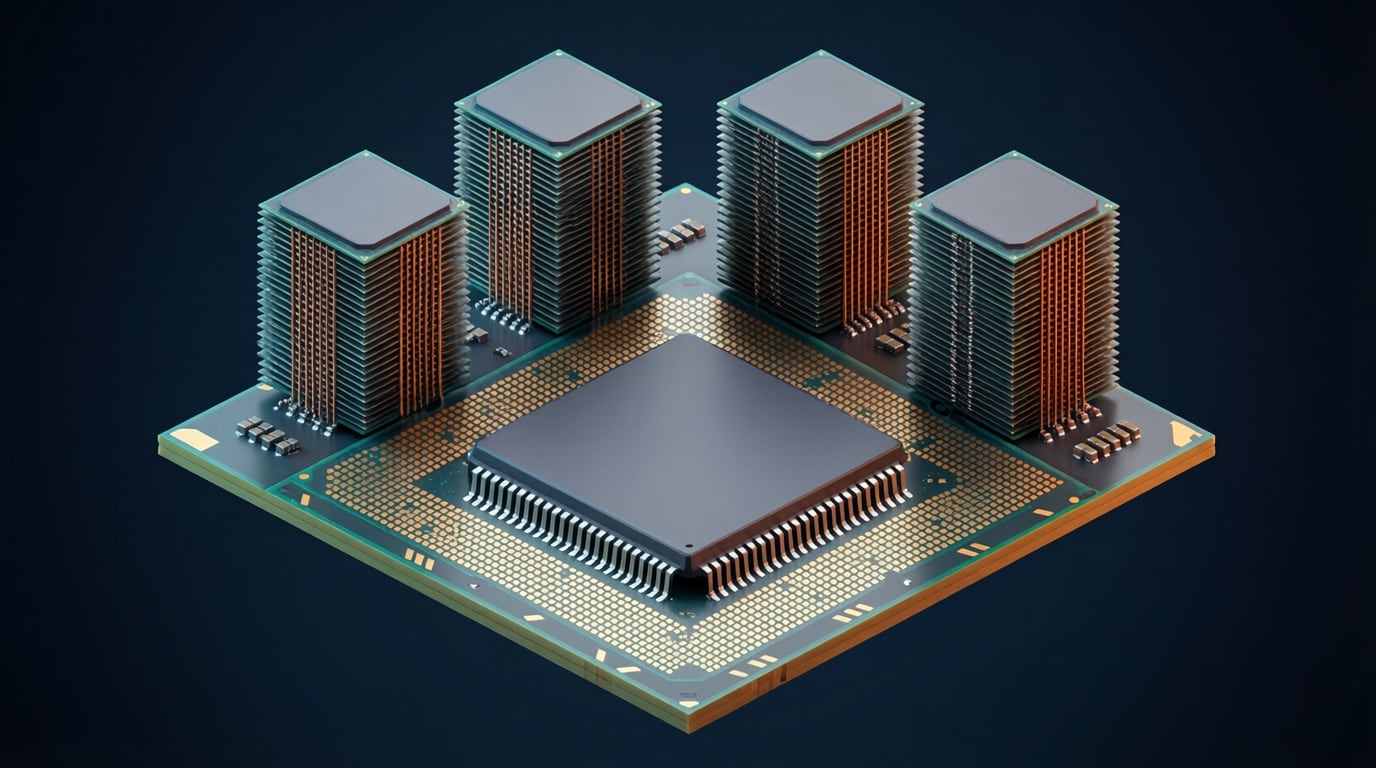
HBM stands for high-bandwidth memory. It is DRAM, but built as a vertical stack of chips that sits within a millimeter of a GPU or AI accelerator and talks to it over a very wide connection. Our glossary entry gives the one-paragraph version. This guide goes further, using only primary sources: the JEDEC standards that define each generation, the spec pages Nvidia and AMD publish for their accelerators, and what Micron, SK hynix and Samsung say in their own product pages, filings and earnings releases.
TL;DR
- What it is: a stack of DRAM dies joined by through-silicon vias (TSVs), mounted next to the processor in the same package. JEDEC’s HBM4 standard (JESD270-4) specifies a 2,048-bit interface, up to 8 Gb/s per pin and up to 2 TB/s per stack.
- Why AI uses it: accelerators need very high memory bandwidth. Nvidia lists 141 GB of HBM3e at 4.8 TB/s for the H200; AMD lists 288 GB of HBM3E at 8 TB/s for the MI355X.
- Who makes it: the three main makers are Micron, SK hynix and Samsung. All three say their HBM4 is in volume production or shipping. Micron says agreements cover “the vast majority” of its calendar 2027 HBM bit supply.
What HBM is
Most memory chips are laid out side by side on a circuit board, apart from the processor. HBM stacks them instead and moves the stack into the processor’s package. Micron contrasts the two designs: a DDR5 module uses a narrower bus at very high clock speeds, while HBM uses a wide, highly parallel interface.
Micron’s HBM FAQ puts the comparison in numbers. A single Micron HBM cube has a 1,024-bit data interface, which Micron says is 16 times wider than a standard DDR5 module. HBM is also placed inside the same package as the CPU or GPU, on a silicon interposer, which shortens the distance data travels. Micron’s 10-Q describes HBM as a 3D stacked DRAM design that uses TSV connections to reach “a higher bandwidth while consuming less power compared to other memory types.”
JEDEC, the industry body that publishes memory standards, defines HBM. In each of the four JEDEC press releases in the table below, the peak bandwidth per stack is higher than in the one before, from faster pins (2018, 2022) or faster pins plus a wider interface (2025). Maximum capacity rose from 8 GB (2016) to 64 GB (2022) through taller stacks and denser dies; HBM4 keeps the same 64 GB maximum (32Gb dies, 16-high).
How it’s built: dies, TSVs, base die and interposer
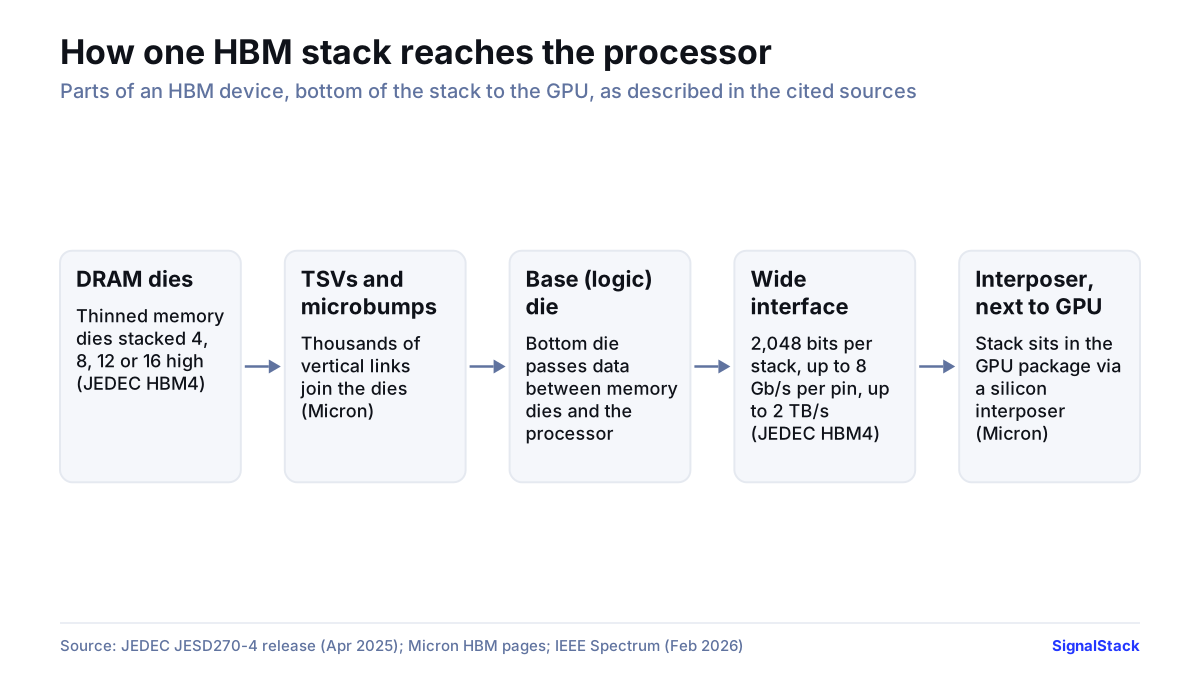
An HBM device, often called a stack or cube, has four parts:
- DRAM dies. Thinned memory chips stacked on top of each other. IEEE Spectrum wrote in February 2026 that stacks then in use had as many as 12 dies; JEDEC’s HBM4 standard allows 4, 8, 12 or 16, and SK hynix’s product page now lists 16-high HBM4.
- TSVs. Vertical electrical connections that pass through each die. Micron says the dies are linked by “thousands” of TSVs and microbumps.
- Base (logic) die. The bottom layer, which passes data between the memory dies and the processor. Micron describes building HBM from three wafer types: DRAM dies with TSVs, thicker top dies without TSVs, and logic dies with TSVs. Samsung says its HBM4 uses a 4nm logic base die.
- Interposer and package. The finished stack sits beside the GPU in one package. Micron says HBM connects to the CPU or GPU through a silicon interposer. IEEE Spectrum reports that stacks sit within a millimeter of the processor and connect through as many as 2,048 micrometer-scale links.
Because of this structure, HBM is harder to make than ordinary DRAM. Micron’s 10-Q lists “achieving acceptable yields and quality for HBM products with their multiple chip layers” among its technology barriers. It also says HBM needs more wafers and more cleanroom space than conventional DRAM to produce the same number of bits on the same technology node.
HBM vs DDR5 vs GDDR7
The table compares the figures in JEDEC’s press release for each memory type’s standard (DDR5 JESD79-5C, GDDR7 JESD239, HBM4 JESD270-4), plus Micron’s FAQ. The three standards are measured differently (per module, per device and per stack), so the rows are not like-for-like on every line.
| DDR5 | GDDR7 | HBM4 | |
|---|---|---|---|
| JEDEC standard | JESD79-5C (Apr 2024) | JESD239 (Mar 2024) | JESD270-4 (Apr 2025) |
| Uses named in the source | Servers, AI and machine learning (JEDEC); system memory for CPUs (Micron) | Graphics, gaming, compute, networking, AI | Generative AI, HPC, high-end graphics cards, servers |
| Data width | 64 bits per module (1/16 of a 1,024-bit HBM cube, per Micron) | 4 independent channels per device | 2,048 bits per stack |
| Speed | Timing parameters defined up to 8,800 Mbps | PAM3 signaling (3 bits over 2 cycles) | Up to 8 Gb/s per pin |
| Bandwidth stated by JEDEC | Not stated in the release | Up to 192 GB/s per device | Up to 2 TB/s per stack |
| Voltages stated by JEDEC | Not stated in the release | Not stated in the release | VDDQ 0.7–0.9V, VDDC 1.0 or 1.05V |
Sources: JEDEC releases for JESD79-5C (Apr 17, 2024), JESD239 (Mar 5, 2024) and JESD270-4 (Apr 16, 2025); Micron HBM and HBM4 pages. The 64-bit DDR5 figure is our arithmetic from Micron’s “16 times wider” statement. Micron says the wide interface lets HBM move data “at much lower energy per bit.”
The generations, per JEDEC
JEDEC published its early HBM standards as updates to one document, JESD235, and HBM3 and HBM4 as new documents. The table uses the figures in JEDEC’s press releases. Each release states peak figures; actual products may differ.
| JEDEC document (release date) | Interface per stack | Per-pin rate | Bandwidth per stack | Stack heights | Max capacity per stack |
|---|---|---|---|---|---|
| JESD235A (Jan 2016) | 1,024-bit, 8 channels | Not stated (2.0 Gb/s by our arithmetic) | 256 GB/s | 2, 4, 8-high | 8 GB |
| JESD235B (Dec 2018) | 1,024-bit, 8 channels | 2.4 Gb/s | 307 GB/s | 2, 4, 8, 12-high | 24 GB |
| JESD238 HBM3 (Jan 2022) | 16 channels of 64 bits (32 pseudo channels) | 6.4 Gb/s | 819 GB/s | 4, 8, 12-high, with provision for 16 | 64 GB (32Gb dies, 16-high) |
| JESD270-4 HBM4 (Apr 2025) | 2,048-bit, 32 channels | 8 Gb/s | 2 TB/s | 4, 8, 12, 16-high | 64 GB (32Gb dies, 16-high) |
Sources: JEDEC press releases of Jan 12, 2016; Dec 17, 2018; Jan 27, 2022; Apr 16, 2025. The 64-bit HBM3 channel width is from JEDEC’s JESD238B.01 document page. JEDEC’s current JESD235 version is JESD235D (Mar 2021); its HBM3 document is now JESD238B.01 (Apr 2025) and its HBM4 document is JESD270-4A, version 1.1 (Dec 2025). We could not read those later revisions, which require JEDEC registration or purchase.
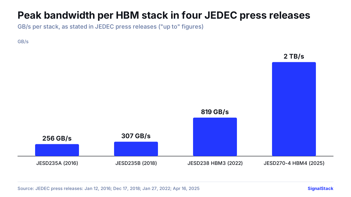
Two points the table shows. First, the HBM3 release says HBM3 doubled the per-pin data rate of the HBM2 generation and its channel count (8 to 16). Halving 6.4 Gb/s gives 3.2 Gb/s for HBM2, above the 2.4 Gb/s in JESD235B (our arithmetic); we found no JEDEC press release for the later JESD235 revisions, up to JESD235D. Second, HBM4 doubled the interface to 2,048 bits and the channels to 32, and JEDEC says the HBM4 interface stays backward compatible with existing HBM3 controllers, so one controller can work with both if needed.
Where is HBM3E? We found no separate JEDEC press release for HBM3E. The three makers sell it as the step between HBM3 and HBM4, and their own product pages give the figures:
| Maker (product page) | HBM3E | HBM4 |
|---|---|---|
| Micron | Over 9.2 Gb/s; over 1.2 TB/s; 24 GB 8-high and 36 GB 12-high | Over 11 Gb/s; over 2.8 TB/s; 36 GB 12-high in high-volume production |
| SK hynix | 9.6 Gbps and higher; 1.23 TB/s and higher; 8/12-high; 24–36 GB | 11.0 Gbps and higher; 2.8 TB/s and higher; 8/12/16-high; 24–48 GB |
| Samsung | Up to 9.2 Gbps; up to 1,180 GB/s; 8/12-high; 24 or 36 GB | Up to 13.0 Gbps; up to 3,300 GB/s; 12-high; 36 GB |
Sources: Micron, SK hynix and Samsung HBM product pages, read Oct 2, 2026.
Every maker’s HBM4 page lists a pin speed above the 8 Gb/s in JEDEC’s April 2025 release (the December 2025 revision may differ; we could not read it). Samsung’s February 2026 release says its HBM4 runs at 11.7 Gbps, “exceeding the industry standard of 8Gbps by approximately 46%.”
Which AI chips use how much HBM
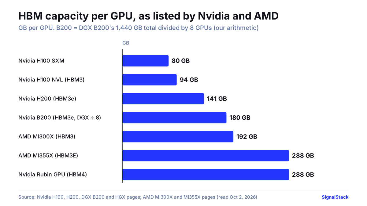
Vendor spec pages give memory per GPU and total memory bandwidth. The table lists what each page states, read on Oct 2, 2026.
| Accelerator | HBM capacity | Memory bandwidth | Memory type stated |
|---|---|---|---|
| Nvidia H100 SXM | 80 GB | 3.35 TB/s | Not stated in the spec table |
| Nvidia H100 NVL | 94 GB | 3.9 TB/s | HBM3 |
| Nvidia H200 | 141 GB | 4.8 TB/s | HBM3e |
| Nvidia B200 (DGX B200 system ÷ 8) | 180 GB | 8 TB/s | HBM3e |
| Nvidia Rubin GPU | 288 GB | 22 TB/s | HBM4 |
| AMD Instinct MI300X | 192 GB | 5.3 TB/s | HBM3 |
| AMD Instinct MI355X | 288 GB | 8 TB/s | HBM3E |
Sources: Nvidia H100, H200, DGX B200 and HGX pages; AMD MI300X and MI355X pages. The B200 row is our arithmetic: Nvidia lists DGX B200 with eight Blackwell GPUs, “1,440 GB total” and 64 TB/s of HBM3e bandwidth. Nvidia’s HGX page lists 1.4 TB of total memory for HGX B200.
Some figures line up with the memory makers’ stacks. AMD lists an 8,192-bit memory interface for the MI300X, the width of eight 1,024-bit HBM3 interfaces (our arithmetic). IEEE Spectrum reports that AMD’s MI350 uses eight 12-die stacks, and Micron says its 36 GB 12-high HBM3E is integrated into the MI350X series; eight 36 GB stacks make 288 GB (our arithmetic). Nvidia says the H200 was the first GPU with HBM3E.
Why so much? IEEE Spectrum explains that memory bandwidth limits how fast large language models can run, and calls the barrier the “memory wall.” In Scientific American, Columbia University professor Keren Bergman says capacity is a problem too: the memory close to the processor is “one or two orders of magnitude less than what you need.”
Who makes it and what they’ve said
Micron (US). In its fiscal Q4 2026 prepared remarks (Sept 30, 2026), Micron said HBM revenue “grew faster than total company revenue.” It said it had completed agreements for “the vast majority” of its calendar 2027 HBM bit supply, with significant price increases from a year earlier. Micron said it expects industry HBM bit shipments “to grow faster than conventional DRAM through calendar 2028.” It also expects initial output from its Singapore HBM packaging facility in early calendar 2027, and says it is working with Nvidia on a custom HBM4E called NVHBM. Our Micron fiscal Q4 2026 report covers the filing in full; see also Micron earnings and the Micron company hub.
SK hynix (KRX: 000660). In its 2Q26 results (July 29, 2026), SK hynix said HBM4 mass shipments started in the second quarter, with a production ramp to follow in the second half. It said it completed HBM4E sample shipments in the first half, and that it has finalized long-term agreements with around 10 customers (the release does not say they cover HBM only). CNBC described SK hynix in 2025 as Nvidia’s main HBM supplier. For SK hynix’s recent DART filings, see our report on its Japan fab, Chongqing sale and Solidigm filings.
Samsung Electronics (KRX: 005930). On February 12, 2026, Samsung said it had begun mass production of HBM4 and shipped commercial products to customers. It anticipated that its HBM sales would “more than triple in 2026 compared to 2025.” In its Q2 2026 results (July 30, 2026), Samsung said it scaled up HBM4 sales and shipped what it calls the industry’s first HBM4E samples. It also said its foundry business benefited from HBM base-die demand.
On market share, CNBC reported on September 30, 2026 that Micron holds the smallest HBM share of the three. None of the three companies gives a share figure in the sources above.
What could change
These are facts and company statements to follow, not predictions.
- Supply. Samsung’s memory business expects HBM, server DRAM and eSSD demand growth to accelerate in the second half of 2026, which it projects will keep the market undersupplied. Micron says it does not have line of sight to when DRAM supply and demand will return to balance.
- Demand risk. Micron’s 10-Q says the long-term trajectory of generative AI, which has driven HBM demand, “is unknown” and that associated demand “may fluctuate.” If HBM demand weakens and makers shift capacity back to conventional DRAM, it warns of possible oversupply.
- Cost. IEEE Spectrum cites a SemiAnalysis estimate that HBM generally costs three times as much as other memory types and makes up 50% or more of a packaged GPU’s cost.
- Next generations. Samsung’s product page lists HBM4E with up to 64 GB and 4 TB/s in a 16-high stack. Micron and Samsung both describe custom HBM work; Samsung said in February that custom HBM samples will start reaching customers in 2027.
- Packaging. In July 2026 JEDEC published JESD330-4 (SPHBM4). It uses the same DRAM dies as HBM4 but a new base die that mounts on standard organic substrates instead of silicon ones. To reach the same bandwidth with 512 data signals instead of HBM4’s 2,048, it uses 4:1 serialization.
- Trade rules. Rest of World notes that the US restricted China’s access to HBM in 2024.
More coverage: AI & Semiconductors.
FAQ
Q What does HBM stand for?
A High-bandwidth memory. It is stacked DRAM, defined by JEDEC standards (JESD235, JESD238 for HBM3 and JESD270-4 for HBM4), that sits in the same package as a GPU or AI accelerator.
Q Why is HBM used for AI?
A IEEE Spectrum calls memory bandwidth a key limiter on how fast large language models run. One HBM4 stack offers up to 2 TB/s under the JEDEC standard, and vendors list 4.8 TB/s of memory bandwidth for Nvidia's H200 and 8 TB/s for AMD's MI355X.
Q Who makes HBM?
A IEEE Spectrum senior editor Samuel K. Moore refers to Micron, Samsung and SK hynix as the "big three" HBM companies. All three list HBM3E and HBM4 on their product pages and say their HBM4 is in volume production or shipping.
Q What is the difference between HBM3E and HBM4?
A HBM4 doubles the interface from 1,024 to 2,048 bits per stack. JEDEC's HBM4 standard specifies up to 2 TB/s per stack; makers list their HBM3E at about 1.2 TB/s per stack and their HBM4 at more than 2.8 TB/s (Micron, SK hynix) or up to 3.3 TB/s (Samsung).
Q How much HBM does an Nvidia B200 have?
A Nvidia lists the eight-GPU DGX B200 with 1,440 GB of HBM3e in total and 64 TB/s of bandwidth. That works out to 180 GB and 8 TB/s per B200 GPU (our arithmetic).
Companies in this report: Micron , NVIDIA , SK hynix , Samsung Electronics
Sources
- JEDEC releases JESD270-4 HBM4 standard (Apr 16, 2025)
- JEDEC publishes JESD238 HBM3 standard (Jan 27, 2022)
- JEDEC updates HBM standard, JESD235B (Dec 17, 2018)
- JESD235 High Bandwidth Memory (HBM) DRAM, document page
- JEDEC updates HBM standard, JESD235A (Jan 12, 2016)
- JEDEC publishes JESD330-4 SPHBM4 standard (Jul 13, 2026)
- JESD270-4A High Bandwidth Memory (HBM4) DRAM, document page
- JESD238B.01 High Bandwidth Memory (HBM3) DRAM, document page
- JEDEC publishes GDDR7 standard JESD239 (Mar 5, 2024)
- JEDEC updates JESD79-5C DDR5 SDRAM standard (Apr 17, 2024)
- NVIDIA H100 Tensor Core GPU specifications
- NVIDIA H200 GPU specifications
- NVIDIA DGX B200 specifications
- NVIDIA HGX platform specifications (Rubin, B300, B200)
- AMD Instinct MI300X accelerator specifications
- AMD Instinct MI355X GPU specifications
- High-bandwidth memory (HBM) product page and FAQ
- Micron HBM3E product page
- Micron HBM4 product page
- Micron Fiscal Q4 2026 Earnings Call Prepared Remarks (Sep 30, 2026)
- Micron Form 10-Q for the quarter ended May 28, 2026
- SK hynix HBM product lineup
- SK hynix Announces 2Q26 Financial Results (Jul 29, 2026)
- Samsung HBM product lineup
- Samsung Ships Industry-First Commercial HBM4 (Feb 12, 2026)
- Samsung Electronics Announces Second Quarter 2026 Results (Jul 30, 2026)
- How and When the Memory Chip Shortage Will End
- AI Is Insatiable (Apr 6, 2026)
- Why high-bandwidth memory is a bottleneck for AI chips
- AI is dominating the world's memory chips. An explainer
- Nvidia-supplier SK Hynix readies production for cutting-edge HBM4 memory chips
- Micron beats on earnings and issues strong guidance as data center revenue jumps 11-fold